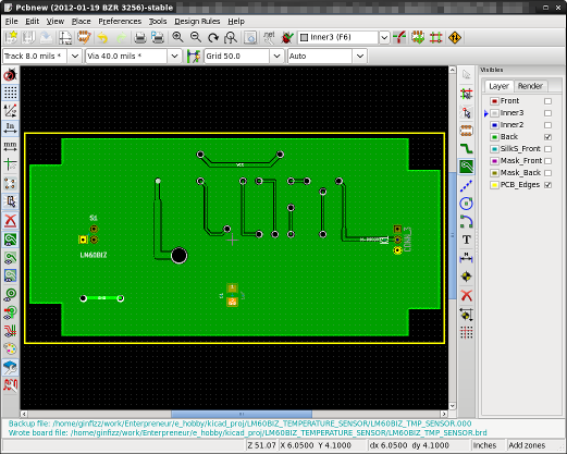
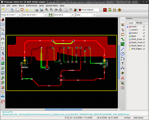
まず、できあがった配線パターンがこれ↓↓↓
で、電グラのベタパターンを生成させるには、まず右側
 ボタンを押す。
押すと、こんなDialogが表示される。
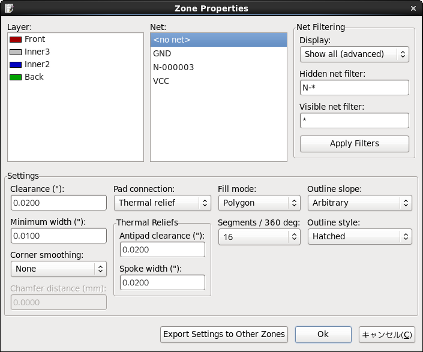
まず、Front layerとVDDを選択して[OK]を押してDialogが閉じた状態で
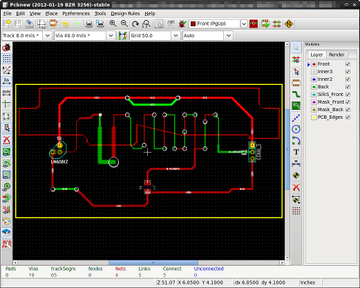
VDDをベタパターン状態にしたい領域を囲ってみると以下のようにハッチング表示される。
 ボタンを押していうr状態で画面上でマウス右クリックしてポップアップメニューを開いて
[Fill or Refill All Zones]を選択すると、
これを
| Front layer | :VDDベタとGNDベタ |
| Inner3 layer | :VDDベタのみ |
| Inner2 | :GNDベタのみ |
| Back layer | :GNDベタのみ |
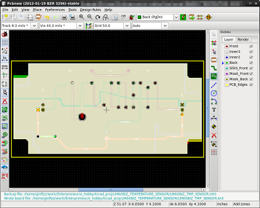
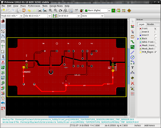
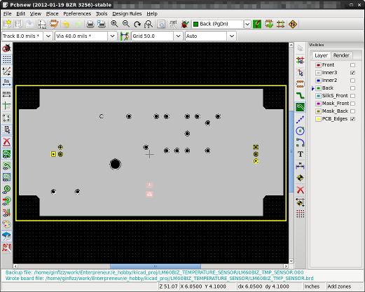
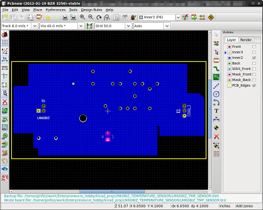
その結果の全layer表示がこれ
-
全layer表示
-
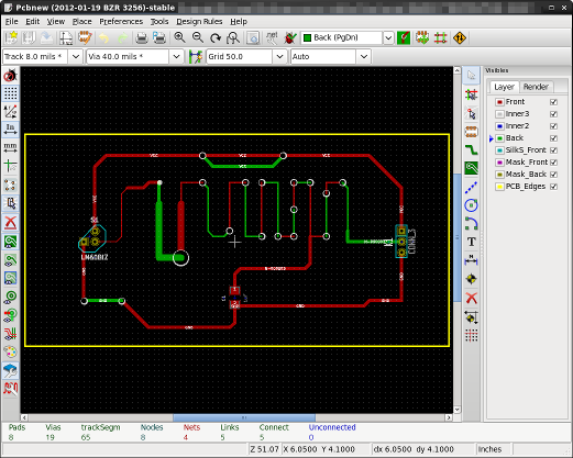
Front layerとPCB_Edgeを表示
-
Inner3 layerとPCB_Edgeを表示
-
Inner2 layerとPCB_Edgeを表示
-
back layerとPCB_Edgeを表示